Saturday, 14 July 2012

Bridge Rectification


It is use the most frequently used circuit in electronic DC power supplies. It converts the full cycle of AC in to DC.
Four diodes and a transformer are used in it. Since, the whole secondary winding of transformer is used in this circuit, so it produces double volts than full wave centre tapped rectifier.
Working Principle
The input of transformer is provided an AC supply.
When the input gets a positive half cycle, the upper end ‘A’ of secondary winding becomes positive and lower end ‘B’ becomes negative. In this condition the diodes D1 and D3 become forward biased and switch to ON condition. And the diodes D2 and D4 are reversed biased and switched to OFF condition. The conventional current starts from point ‘A’ and travels through D1 load and D3 to complete its circuit.( As shown in figure 1).


Figure 1
When the input gets negative half cycle then point ‘A’ becomes negative and point ‘B’ becomes positive. In this condition, the diodes D2 & D4 are forward biased and switched to ON condition. While the diodes D1 & D3 become reverse biased and switched to OFF condition. The current starts from point ‘B’ travels through D2 , load and D4 to complete its circuit. (Shown in figure 2).


Figure 2

Full wave rectifier

A device that converts both polarities (positive and negative) of input AC into output DC is know asFull Wave Rectifier. OR
A rectifier that converts complete cycle of input AC into output DC is known as Full-wave Rectifier.
Full Wave Rectifier (Circuit Diagram and Output)
 When the positive half cycle comes, then upper end ‘A’ of secondary winding becomes positive and lower end ‘B’ becomes negative while central point ‘G’ remains at zero potential. In this condition the diode D1is forward biased and conducts, while the diode D2 is reversed biased and switched to OFF condition and doesn't conduct.
Conventional current travels from point ‘A’ through diode D1 and reaches center tap point ‘G’ of transformer, Hence during positive half cycle D1 is ON and D2 remains OFF. (As shown in figure1)
Figure 1 (Output of Diode D1)
 When the negative half cycle comes, then upper point ‘A’ of secondary winding becomes negative and lower point ‘B’ becomes positive while central point ‘G’ remains at zero potentioal. In this condition, the diode D2 conducts because it is forward biased and the diode D1 is reverse biased and doesn’t conduct.
Conventional current travels from point ‘B’ towards load and reaches the center taps point ‘G’ of secondary winding. Hence, during negative half cycle D1 is Off and D2 is ON. (As shown in figure 2).

Half wave rectifier


Half-wave rectifier. OR
A device that converts half-cycle of input AC into output DC is known as Half-wave Rectifier.
As shown in the figure below.
circuit diagram of half wave rectifier
Half Wave Rectifier (Circuit Diagram)
When the positive half cycle of input AC wave comes, than the diode is forward biased and switched into ON condition, So it conducts and positive half-cycle of input AC is dropped across RL.
When the negative half cycle of input AC comes, the diode is reverse biased and switched to OFF condition. Thus the diode doesn’t conduct and no voltage is dropped across RL. So negative half cycle is skipped.
So, the output is not a steady DC but a pulsating DC, having a specific frequency equal to that of the input voltage frequency.
Since only half cycle of input wave is used, it is called half wave rectifier.
If it is required to step up or step down the input voltage, we will have to use a power transformer as shown in figure, below.
Power Transformer (Step-up action)

NPN Transistors


Definition:
A transistor in which a P-type semiconductor is sandwiched between tow N-type semiconductors, is known as NPN transistor.
NPN is one of the two types of bipolar transistors, consisting of a layer of P-doped semiconductor (the "base") between two N-doped layers. (As shown in the Diagram)


npn transistor muftarticles
NPN Transistor
In this type of transistor, a small amount of current flows because P-region(Base) has a small amount of charge carriers.
The holes move from base towards emitter, they cannot go towards collector because collector has smaller amount of charge carriers as compared to emitter.


symbol of npn transistor
Symbol of NPN (Circuit Diagram)

Transistors

Definition:
"A transistor is a semiconductor device used to amplify andswitch electronic signals and power. It is composed of a semiconductor material with at least three terminals for connection to an external circuit." 
A voltage or current applied to one pair of the transistor's terminals changes the current flowing through another pair of terminals. Because the controlled (output) power can be much more than the controlling (input) power, a transistor can amplify a signal.
The transistor is the fundamental building block of modern electronic devices.


symbol and construction of a Transistor on muftarticles


Usage:
The bipolar junction transistor (BJT) was the most commonly used transistor in the 1960s and 70s. Even after MOSFETs became widely available, the BJT remained the transistor of choice for many analog circuits such as simple amplifiers because of their greater linearity and ease of manufacture. Desirable properties of MOSFETs, such as their utility in low-power devices, usually in the CMOS configuration, allowed them to capture nearly all market share for digital circuits; more recently MOSFETs have captured most analog and power applications as well, including modern clocked analog circuits, voltage regulators, amplifiers, power transmitters and motor drivers.
Most common uses of transistors are:

1.Transistor as a switch

2. Transistor as an Amplifier

Types:

Transistors are categorized by

  • Semiconductor material: graphene, germanium, silicon, gallium arsenide, silicon carbide, etc.
  • Structure: BJT, JFET, IGFET (MOSFET), IGBT, "other types"
  • Polarity: NPN, PNP (BJTs); N-channel, P-channel (FETs)
  • Maximum power rating: low, medium, high
  • Maximum operating frequency: low, medium, high, radio frequency (RF),microwave (The maximum effective frequency of a transistor is denoted by the term fT, an abbreviation for "frequency of transition". The frequency of transition is the frequency at which the transistor yields unity gain).
  • Application: switch, general purpose, audio, high voltage, super-beta, matched pair
  • Physical packaging: through hole metal, through hole plastic, surface mount,ball grid array, power modules
  • Amplification factor hfe (transistor beta)

Biasing and Working of NPN Transistors


Due to forward biasing of emitter-base junction, majority carriers (Electrons) flow towards base. A big amount of electrons cross the junction and enter the base. As the base is lightly doped, so a small amount (2 to 5 percent) of electrons recombine with holes in the base and almost more than 95 percent electrons come under the effect of positively charged collector and enter the collector. This is possible due to attraction of collector voltage.
As collector-base junction is reverse biased, so electrons cannot flow from collector to base due to high resistance, infect, electrons always flow from base to collector.
 Thus due to diffusion and collection of electrons (provided by emitter) in the collector-base junction, the flow of electronic current starts. The direction shown in figure shows the flow of conventional current.
This should be kept in mind that the transistor will not conduct unless its emitter-base junction is forward biased.
Figures,


biasing of NPN transistor
Biasing of NPN Transistor


circuit diagram of NPN transistor
Biasing of NPN Transistor (Symbol, Circuit Diagram)


PNP Transistor


A transistor in which an N-type semiconductor is sandwiched between tow P-type semiconductors, is known as PNP transistor. (Shown in Figure)
diagram of pnp transistor muftarticles
In the p-region, majority carriers are holes or protons, and in the n-region, majority carriers are electrons.


circuit diagram of pnp transistor on muftrarticles
Symbol of PNP Transistor
As conventional current flows in the transistors, so charge carriers start moving from emitter and they are collected at collector.

Biasing and Working of PNP Transistor


For the normal operation of a transistor, it is necessary to provide voltage of right polarities to both of its junctions.
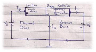
For the accurate and normal function of a transistor, its emitter-base junction should be forward biased and collector-base junction should be always reverse biased. As shown in the figure.
biasing of PNP transistor muftarticles


circuit diagram of PNP transistor muftarticles

In the given method of biasing of PNP transistor, the emitter-base junction is forward biased, while collector-base junction is reverse biased.
Due to forward biasing of emitter-base junction, the majority carriers (holes) flow from emitter towards base. Thus, a big amount of holes crosses the junction and enters base. As the holes enter the base, they combine with electrons present there, (This process known as recombination).Since the base is lightly doped, so the recombination of holes and electrons in base is very low, (Almost 2% to 5%). Thus 95 to 98 percent of holes that came from emitter could not recombine with electrons.

Since the collector-base junction is reverse biased, so holes cannot flow from collector to base due to high resistance. But holes start to flow in the opposite direction (i.e. base to collector) because collector voltage attracts almost 95% holes present in base region. Thus the holes provided by emitter, travelling through base, go to collector-base junction and conventional current starts to flow in PNP transistor.
This should be kept in mind that collector current and emitter current is almost equal but base current is very low. 

Common Emitter (CE) Amplifier


When a transistor is added to a circuit such that, input signal is provided parallel to its emitter-base junction and output is obtained from collector-emitter junction while emitter is common or grounded then such circuit is called common-emitter circuit. This circuit is the most popular method to use transistor as an amplifier.
In other words, “common-emitter circuit” is a circuit in which:
        1.     Emitter is grounded
        2.     Input signal is provided across base
        3.     And output signal is obtained across collector
A signal stage CE amplifier circuit is shown, in the figure, in which NPN transistor is used.
Base is ‘driven element’ in it (it means that base current plays the role of input)
 Input current is provided through base-emitter circuit while, output signal is obtained through collector-emitter circuit.
Emitter base junction is forward biased with battery VB and collector-base junction is reverse-biased with battery VCC

Circuit Operation of Common Emitter (CE) Amplifier


When the positive half-cycle of signal is provided
(1)             As the base of transistor is already positive relating to biasing, so voltage (VBC) increases.
(2)             Due to increase in VBE , the forward bias of Emitter-base junction also increases.
(3)             Iis also slightly increased.
(4)             As a result of increase in IB (Base Current), the I(Collector Current) increase up to B times as (IC = BIB).
(5)             Due to increase of I, a large increase in ICRdrop occurs.
(6)             VCE decreases according to following equation.
VCE = VCCICRC
Thus, negative half-cycle of input is achieved. It means that when positive input signal is provided to such circuit, then the amplified output signal is negative, (as shown in figure)
When negative half-cycle is provided to input then the achieved output cycle is positive.

Characteristics of a Common Emitter (CE) Amplifier


(1)             Its input resistance is less up to a specific limit (1K to 2K)
(2)             Its output resistance is high up to a proper limit (50K or above)
(3)             Its current gain (B) is high (50 to 300 times)
(4)             Its voltage gain is very high (1500 or more)
(5)             It produces a big power gain (10,0000 times or 40 db)
(6)             It produces “Phase Reversal” of input signal. It means that input signal and output signal are produced at a difference of 180 degree to each other.
Related:
Common Emitter (CE) Amplifier
Circuit Operation of Common Emitter (CE) Amplifier

Introduction to Digital Electronics


Digital electronics is one of the fundamental courses found in all electrical
engineering and most science programs. The great variety of LabVIEW
Boolean and numeric controls/indicators, together with the wealth of
programming structures and functions, make LabVIEW an excellent tool to
visualize and demonstrate many of the fundamental concepts of digital
electronics. The inherent modularity of LabVIEW is exploited in the same
way that complex digital integrated circuits are built from circuits of less
complexity, which in turn are built from fundamental gates. This manual
is designed as a teaching resource to be used in the classroom as
demonstrations, in tutorial sessions as collaborative studies, or in the
laboratory as interactive exercises.
The order of the labs follows most electronic textbooks. The first six labs
cover the fundamental circuits of gates, encoders, binary addition,
D-latches, ring counters, and JK flip-flops. Many of the VIs are suitable for
both classroom demonstration and laboratory exploration.
The second set of six labs cover advanced topics such as DACs, ADCs,
seven-segment displays, serial communication, and the CPU. These are best
done in the context of a digital electronics lab, comparing the LabVIEW
simulations with real integrated circuits. In each case, you can enhance
simulations presented in the text by using a National Instruments DAQ
board to interact with the real world through LabVIEW digital I/O, analog
out, analog in, and serial VIs.
Labs 2, 5, and 12 are application oriented and are designed to demonstrate
encoding schemes, digital encryption, and the operation of a CPU. These
labs could be presented as challenging problems in a tutorial setting or in a
workshop environment.
The labs can also be grouped to demonstrate special relationships of
advanced devices on certain basic gates. For example, the CPU operation is
dependent on the concept of registers and two input operations.
This manual includes a complete set of LabVIEW VIs. The text is also
included on the CD so that you can customize the material.

The AND Gate


A basic AND gate consists of two inputs and an output. If the two inputs
are and B, the output (often called Q) is “on” only if both A and are
also “on.”
In digital electronics, the on state is often represented by a 1 and the off state
by a 0. The relationship between the input signals and the output signals is
often summarized in a truth table, which is a tabulation of all possible inputs
and the resulting outputs. For the AND gate, there are four possible
combinations of input states: A=0, B=0; A=0, B=1; A=1, B=0; and A=1, B=1.
In the following truth table, these are listed in the left and middle columns.
The AND gate output is listed in the right column.

Table 1Truth Table for AND Gate
A
B
Q=A AND B
0
0
0
0
1
0
1
0
0
1
1
1

In LabVIEW, you can specify a digital logic input by toggling a Boolean
switch; a Boolean LED indicator can indicate an output. Because the AND
gate is provided as a basic built-in LabVIEW function, you can easily wire
two switches to the gate inputs and an indicator LED to the output to
produce a simple VI that demonstrates the AND gate.

LabVIEW AND Function Wired to I/O Terminal Boxes the AND gate muftarticles
                      Figure 1 LabVIEW AND Function Wired to I/O Terminal Boxes

Run AND gate.vi from the Chap 1.llb VI library. Push the two input buttons
and note how the output indicator changes. Verify the above truth table.

The OR and XOR Gates


The OR gate is also a two-input, single-output gate. Unlike the AND gate,
the output is 1 when one input, or the other, or both are 1. The OR gate
output is 0 only when both inputs are 0.

A
B
Q=A AND B
0
0
0
0
1
1
1
0
1
1
1
1


A related gate is the XOR, or eXclusive OR gate, in which the output is 1
when one, and only one, of the inputs is 1. In other words, the XOR output
is 1 if the inputs are different.

How are computers made?

We started by showing the stuff that computers are made of. It all begins with common sand,
which consists mostly of silicon dioxide (quartz). Using chemical methods, the sand is converted
to pure silicon. Very pure silicon, 99.999 999% -- you can’t get anything more pure.
Pure silicon is a funny material. It shines like a metal, but is breakable like a ceramic. It is a
semiconductor. That means it is on the edge: does it conduct electricity or doesn’t it? Well, we
can make it do both: make it conduct, or make it stop conducting.We can switch an electrical
current in silicon on or off, at will, and very, very fast. From silicon, we make fast switches!
A whole bunch of those switches together make a chip, which is put inside a plastic cover.
A bunch of chips are mounted on a printed circuit board.
A bunch of boards make an electronic box: a VCR, a TV, a radio, a computer.
Well, of course you need more stuff, like a power supply, a display, a hard drive, and a box to fit
it all in. But the heart of anything electronic is those silicon switches.

What do computers do?

We use computers for a lot of things. Playing games, writing book reports, calculating math
problems... It actually all started with math problems.
Ÿ So these boxes can calculate quite well. Very well.
Ÿ We do know that they do what they are told. You push a button, and the computer does it.
It does exactly what you tell it to do (which is not necessarily what you meant it to do...).
It follows instructions.
Ÿ Computers move information, for example your book report from the disk to the printer.
Or a file from the Internet to your display screen, or to your own hard disk. They store
information (all the book reports you have written are stored on the hard disk), and they
manage it (you can find it again).
How do those silicon switches we talked about actually make all this happen?
This class is going to explore just that: how we can do cool things, such as writing text, making
pictures and calculating with switches. Just like computers do.
This is called switch logic, or Boolean logic, after George Boole (English mathematician,
1815-1864), who was the first to think of it -- long before electronics existed!